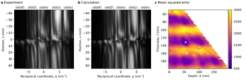
Figure 1: (a) Experimentally obtained momentum resolved STEM data, (b) Calculated data for a dislocation model. (c) Optimization of dislocation model parameters (from Niermann et al., “Three dimensional classification of dislocations from single proj
Development of a new method for the reconstruction of the electrostatic potential of interfaces utilizing momentum resolved STEM
Researcher: Dr. Laura Niermann, Technische Universität Berlin, Institut für Optik und Atomare Physik
Measuring facility: ZELMI: Center for Electron Microscopy (TU Berlin) and Institute of Physics, Structure Research and Electron Microscopy group (HU Berlin)
In her recent work Dr. Laura Niermann utilized dynamical diffraction within momentum resolved STEM measurements to determine the three dimensional strain field from a measurement along a single direction. This newly developed method was already applied to determine the three dimensional position and the type of a dislocation (Fig.1). However, it is not only limited to investigations of the three dimensional strain fields, but can also be developed further for investigations of the electrostatic potential landscape at interfaces, e. g. for characterization of polarization fields at AlGaN / GaN interfaces. In comparison, state of the art S/TEM techniques like differential phase contrast or off-axis electron holography encounter several challenges like the abrupt material change, strain fields at the interface, and dynamical diffraction effects, when measuring such polarization fields.
The aim of the project is the development of a new approach for the reconstruction of the electrostatic potential at interfaces by utilizing dynamical diffraction within momentum resolved STEM measurements. A scheme will be developed that inverts the electron scattering by comparing the expected momentum resolved STEM data calculated from an iteratively optimized description of the electrostatic potential with the experimentally obtained data.
Dr. Laura Niermann’s work allows to quantitatively characterize and further optimize critical interfaces in high performance opto-electronical semiconductor devices. Through the collaboration with the Center for Electron Microscopy (ZELMI, TU Berlin) and AK Koch (HU Berlin) the first groundbreaking steps are made.

