Ptychography-Enabled In-Operando Validation of Semiconductor Nanostructure Models
Researcher: Hüseyin Çelik, Technische Universität Berlin, Institute of Optics and Atomic Physics
Measuring facility: Institute of Physics, Structure Research and Electron Microscopy group (HU Berlin)
Project Overview:
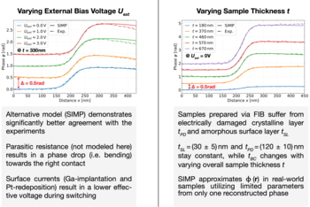
This project, supported by the ACEM, aimed to validate a novel numerical model for predicting three-dimensional electrostatic potential distributions in semiconductor nanostructures. Using ptychography and advanced 4D-STEM methods under in-operando conditions, experiments were conducted on the Nion STEM HERMES 200kV at Humboldt-Universität zu Berlin.
Key Outcomes:
- Successful verification of the model under varying illumination conditions.
- Demonstrated the model’s robustness using state-of-the-art STEM techniques.
- Results have already contributed to a peer-reviewed publication and multiple conference presentations.
Significance:
This project highlights the transformative potential of electron microscopy for semiconductor research, providing insights into dynamic processes at the nanoscale. Access to advanced infrastructure enabled by the ACEM has been pivotal for early career researchers like Hüseyin, fostering success and inspiring future research.

